New student club launches ambitious semiconductor manufacturing project
A new student group at University of Illinois Chicago will be the first in the country to run a novel initiative on the frontier of semiconductor and microsystems manufacturing.
The Semiconductor and Microsystems Manufacturing Club, or SEMMI, brings together students interested in designing and fabricating computer chips and other microelectronic systems. In their first major activity, they’ll lead and fabricate a multi-project wafer shuttle run — a collaborative type of semiconductor and microsystems manufacturing where designs from several academic and industrial partners are combined on a single wafer.
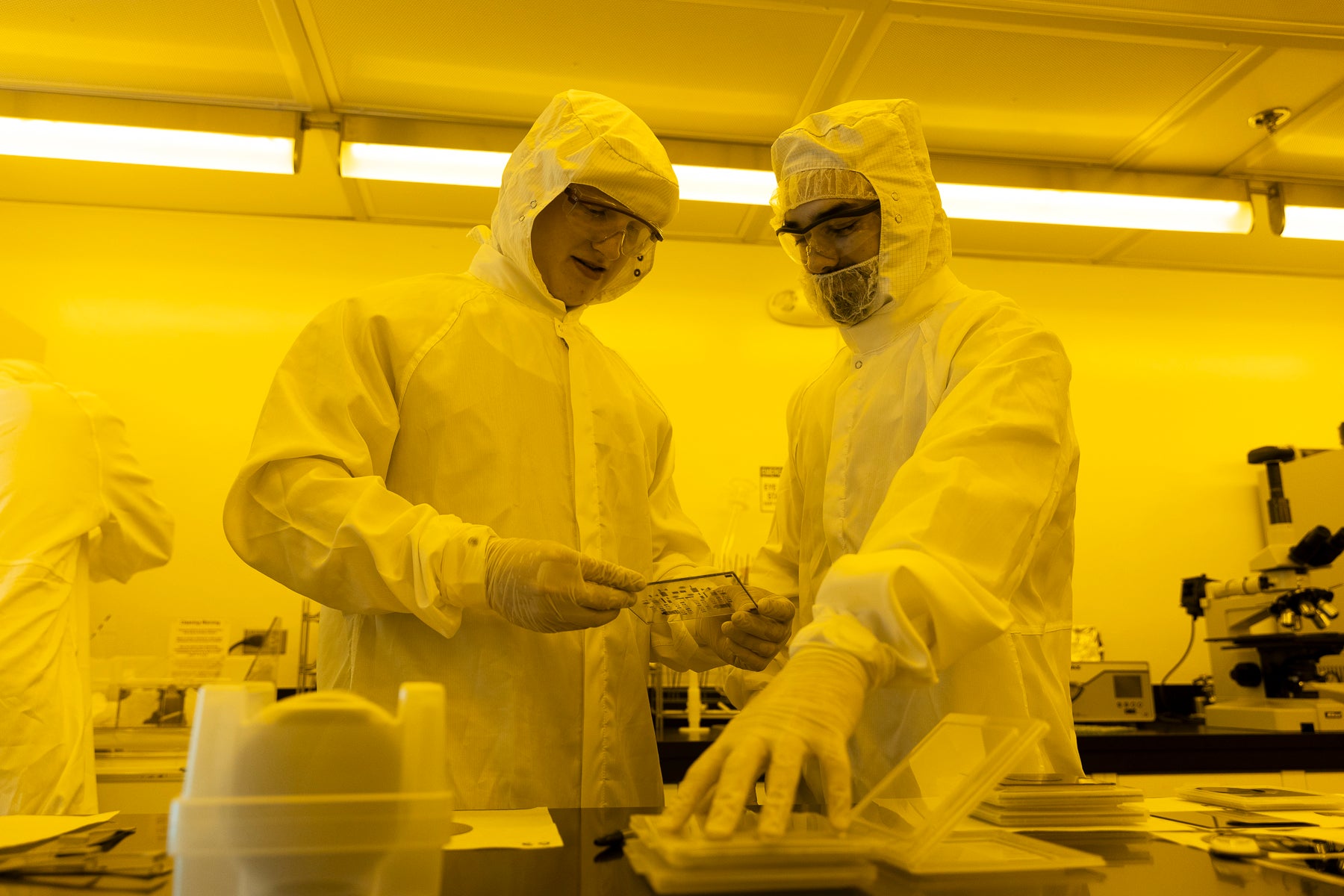
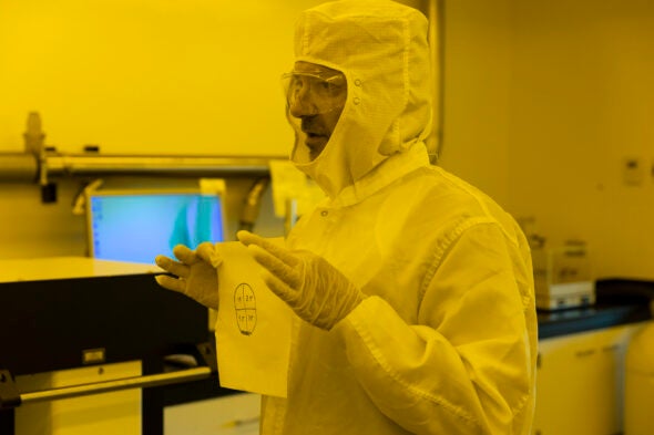
The group formed this year through an initiative in the UIC Department of Electrical and Computer Engineering and grew from a course on fabricating devices such as microsensors, microstructures and microelectronics. In the class, students execute the intricate steps of chip design and fabrication in the Nanotechnology Core Facility, learning many of the techniques currently used by the semiconductor industry.
Through the new club and its multi-project wafer initiative, students will have greater access to this advanced cleanroom facility and more chances to interact with global semiconductor companies.
“There is now a tremendous push for revitalizing domestic manufacturing, and semiconductor manufacturing is a big part of it,” said Igor Paprotny, associate professor in the UIC Department of Electrical and Computer Engineering and Nanotechnology Core Facility research director. “There will be a need for a skilled workforce, and we can really use this momentum to make sure that we have activities, such as the multi-project wafer run, that give students opportunities to boost their leverage when it comes to looking for jobs.”
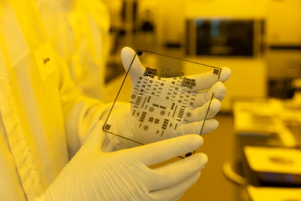
Wafers are thin pieces of silicon used as the main material in microelectronics. If a standard wafer is like a one-topping pizza, with the same microelectronics design replicated many times across its surface, a multi-project wafer is like a pizza with dozens of toppings. The additional design space enables more experimentation and experience working with a broader range of devices.
In previous years, teams of students from the class have fabricated and tested their designs on small wafers. But this spring, the class started using a larger, 4-inch wafer, which has room for around 100 individual segments, called dies. Each die can contain hundreds of devices. This additional die space creates the possibility of new partnerships, where designers outside UIC can contribute their designs to be fabricated on the large wafer alongside student designs.
Multi-project wafers aren’t typically done in academic settings, and the UIC initiative will be even more exceptional as the first entirely student-run activity. The group aims to conduct two runs a year, using processes developed at UIC.
In managing and fabricating the multi-project wafer runs, students will gain skills and foster connections with companies in the high-demand semiconductor manufacturing industry and foster better integrations with partners in the Chicago area and beyond.
“We are advertising the process to outside users, and it will be a great learning experience for our students to manage those interactions,” Paprotny said. “Our aim is to offer die-sites at no cost to community colleges and research institutions that do not have the clean room and the tools we have at UIC. The inaugural run is offered for free to our partners.”
The experience will make UIC students stand out for desirable internships and jobs, said Gabriel Rusecki, who is studying electrical and computer engineering and founded the club.
“As an undergrad, it’s super hard to get your foot into the semiconductor manufacturing industry, so this helps with outreach to companies” Rusecki said. “They might want to come to us because they will see that these students are interested in this section of semiconductor manufacturing and maybe grab them up and hire them as an employee.”
When the wafers are complete, the project will conclude with a friendly competition hosted at UIC. UIC students will test the performance of their microelectronics against each other and designs submitted by outside partners. Besides UIC groups, the University of Maryland and the City Colleges of Chicago Engineering Program will be part of the initial user cohort. This and other student initiatives are also interconnected with UIC’s leading role in the Illinois Semiconductor Workforce Network, funded by the federal CHIPS and Science Act, as well as other CHIPS-related activities.
The club is also ramping up other activities, including outreach to local museums and inviting speakers from the semiconductor industry to campus.
“Engineering and science — it’s all about collaboration, having innovative ideas,” said Nabharun Bhattacharya, a student in the group. “So if you have a student organization and every student is collaborating with each other, that builds up that spirit.”
